Live Chat
Need Help?
Privacy PolicyPower MOSFETs
Small-Signal MOSFETs
We designed our small-signal MOSFET products, also called interface MOSFETs, for low-power, signal-level applications. These applications include signal amplification and level translation, signal bypass, system protection or lower power regulation (voltage and current regulation). These MOSFETs come in resistances from a few hundred to multiple ohms of on-resistance and they are available in a variety of small-footprint packages. You can use these small-signal devices in diverse applications in a varied range of markets from consumer to medical.

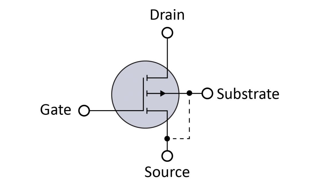
Enhancement-Mode N-Channel MOSFETs
You can use these MOSFETs in a DC-DC converter switch or a linear regulator pass transistor. Their mode is normally off.
High-Voltage Power MOSFETs:

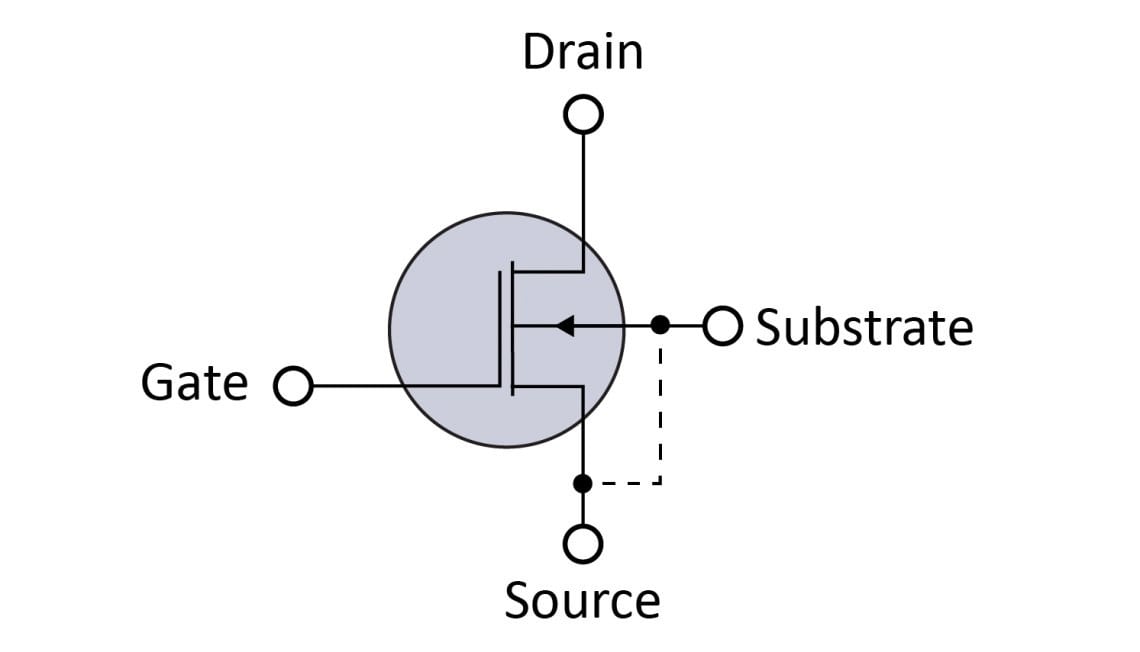
Enhancement-Mode P-Channel MOSFETs
These MOSFETs are well suited for use in the high-side switch of a power converter or in a linear regulator and CMOS switch with N-channel MOSFETs. Their mode is normally off.

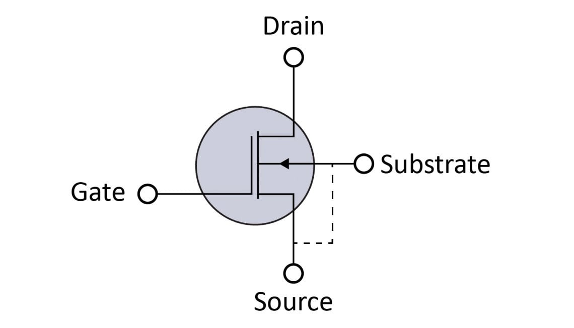
Depletion-Mode N-Channel MOSFETs
You can use these MOSFETs in a start-up circuit of power supply Integrated Circuits (ICs) or a pass transistor for a linear regulator. Depletion-mode MOSFETS are switched on when zero voltage applies across the gate and the source. Their mode is normally on.

N-Channel Enhancement-Mode MOSFET Arrays
You can use these MOSFET arrays in LED-driving circuits, motor controls and relay-driving controllers.

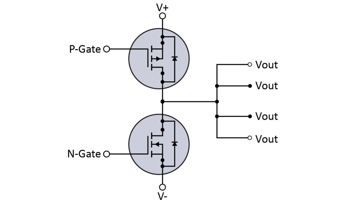
Complementary MOSFET Arrays
You can use these products in motor control circuits or DC-DC converter half-bridge switches.

Radiation-Hardened MOSFETs
Our rad-hard MOSFETs feature low RDS(on) and low total gate charge. These devices have been developed for Total Dose and Single-Event environments.
Enhancement Mode (Normally Off)
MOSFETs use a vertical DMOS structure in power switches combined with a well-proven, rugged gate oxide process. There are two types of enhancement-mode MOSFETs: P channel and N channel. Characteristic of all MOS structures, these devices are free from thermal runaway and thermally induced secondary breakdown. You can use lateral MOSFETs with no intrinsic body diode and often-ballasted source areas for linear mode operation amplifiers, the most prevalent of which are RF power amplifiers (e.g., LDMOS).
Depletion Mode (Normally On)
These transistors also use lateral DMOS technology. The key difference is that the depletion-mode MOSFET is normally on and commanded off when Vgs increases.
N-Channel MOSFETs
N-channel MOSFETs are enhanced when the gate is pulled positive with respect to the source. N-channel MOSFETs tend to have lower RDS(on) per unit area compared to P-channel MOSFETs. In a half-bridge stage, the high-side N-channel MOSFET must have a means of holding the gate voltage positive as the device turns on. This requires a voltage above the rail, which you can derive by using bootstrapped drivers that allow a flying capacitor bank tied to the source of the high-side switch to charge when the low-side switch turns on and then flying up with the source to hold it on or with galvanically isolated drivers.
P-Channel MOSFETs
P-channel MOSFETs are enhanced when the gate is pulled negative with respect to the source. This is often advantageous in a high-side switch application because the circuit does not require an isolated or bootstrapped driver but rather a simple clamp to protect the gate oxide and a pull-down circuit or driver. P-channel MOSFETs have been popular in lower-power high-side switches, hot swap applications on the positive rail, electronic relays, electronic circuit breakers and general DC switching.
- Enhancement-Mode N-Channel
- Enhancement-Mode P-Channel
- Depletion-Mode N-Channel
- N-Channel Enhancement-Mode Arrays
- Complementary Arrays
- High-Voltage Enhancement-Mode N-Channel
- SiC Enhancement-Mode N-Channel

MPLAB® Analog Designer
MPLAB Analog Designer provides design suggestions for common circuit needs, estimates performance for common modifications and exports to MPLAB® Mindi™ Analog Simulator for verification.

MPLAB® Mindi™ Analog Simulator
MPLAB Mindi Analog Simulator uses a SIMetrix/SIMPLIS environment to model circuit behavior, reducing design time with software debugging for initial design verification.

Power Check Design Service
This service offers advice on your exact physical circuit layout, sharing best practices from an experienced power supply designer so that physical hardware will match simulations.